Hybrid and Plasmonic Semiconductor Nanowires & Nanowire Lasers
Emission of Excitons in Hybrid and Plasmonic Nanowires
The coupling of light into the free-electron gas in dielectric/metal nanostructures and films offers unprecedented control over refraction properties and light routing on the nanoscale. High resistivity losses in metal films, however, currently limit the feasibility of many applications. We investigate novel plasmonic structures with integrated semiconductor nanowires as a gain material to compensate for metal losses. We study the physical processes that are responsible for the coherent and incoherent energy-transfer between excitons and plasmons with ultrafast spectroscopic methods and with electron energy loss spectroscopy (EELS) in collaboration with Prof. Duscher, University of Tennessee, Knoxville. Our research attracts attention at international conferences and has led to press releases at the University of Cincinnati and on the internet (see for instance: http://www.uc.edu/news/NR.aspx?id=21271, http://theconversation.com/plasmonics-revolutionizing-light-based-technologies-via-electron-oscillations-in-metals-38697 and http://magazine.uc.edu/editors_picks/recent_features/nanotech.html.)
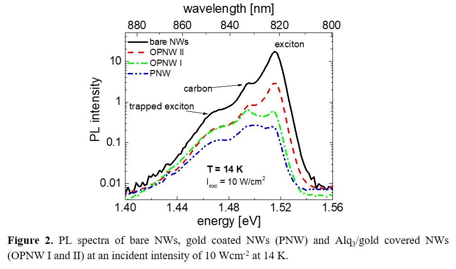
Plasmonic GaAs-AlGaAs-GaAs nanowires (NWs) (see Fig. 1 (b)1) with a ~10 nm thick Au coating (PNW) but without Alq3 spacer layer reveal a significant reduction of the PL intensity of the exciton emission (see Fig. 21) compared with the uncoated NW sample. Plasmonic NW samples with the same nominal Au coverage and an additional Alq3 interlayer of 3 nm (OPNW I) or 6 nm (OPNW II) thickness (see Figs. 1 (c) and (d) show a clearly stronger PL intensity which increases with rising Alq3 spacer thickness. Time-resolved (TR) PL measurements reveal an increase of the exciton decay rate by a factor of up to two with decreasing Alq3 spacer thickness suggesting the presence of Förster energy transfer from NW excitons to plasmon oscillations in the gold film. The weak change of the decay time, however, indicates that Förster energy-transfer is only partially responsible for the PL quenching in the gold coated NWs. The main reason for the reduction of the PL emission is attributed to a gold induced band-bending in the GaAs NW core which causes exciton dissociation. With increasing Alq3 spacer thickness the band-bending decreases leading to a reduction of the exciton dissociation and PL quenching. Our interpretation is supported by electron energy loss spectroscopy (EELS) measurements which show a signal reduction and blue shift of defect (possibly EL2) transitions when gold particles are deposited on NWs compared with bare or Alq3 coated NWs.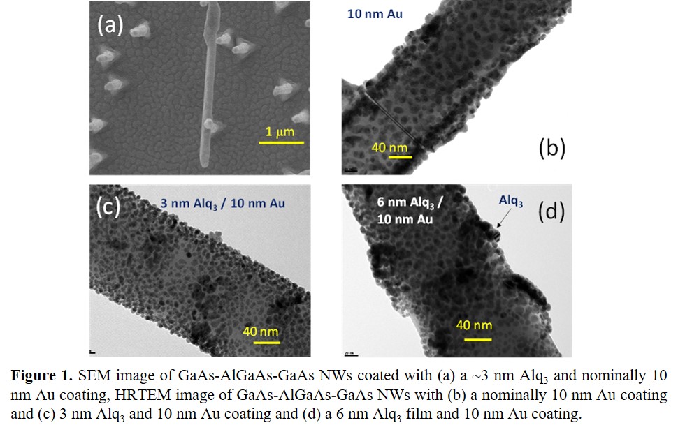
1Reprinted with permission from M. Kaveh, Q. Gao, C. Jagadish, J. Ge, G. Duscher, and H. P. Wagner, Controlling the exciton emission of gold coated GaAs-AlGaAs core-shell nanowires with an organic spacer layer, Nanotechnology 27, 485204 (2016), Copyright 2016, IOP.
We studied the emission of bare and aluminum quinoline (Alq3)/gold coated wurtzite GaN nanorods by temperature- and intensity-dependent time-integrated and time-resolved photoluminescence (PL). The GaN nanorods of ~1.5 micrometer length and ~250 nm diameter were grown by plasma-assisted molecular beam epitaxy. Gold/Alq3 coated GaN nanorods were synthesized by organic molecular beam deposition. The near band-edge and donor-acceptor pair luminescence was investigated in bare GaN nanorods and compared with multilevel model calculations providing the dynamical parameters for electron-hole pairs, excitons, impurity bound excitons, donors and acceptors. Subsequently, the influence of a 10 nm gold coating without and with an Alq3 spacer layer was studied and the experimental results were analyzed with the multilevel model (see Fig. 3 2). Without spacer layer a significant PL quenching and lifetime reduction of the near band-edge emission is found (Fig. 3 (d)). The behaviour is attributed to surface band-bending and Förster energy transfer from excitons to surface plasmons in the gold layer. Inserting a 5 nm Alq3 spacer layer reduces the PL quenching and lifetime reduction (see Fig. 3 (e)) which is consistent with a reduced band-bending and Förster energy transfer. Increasing the spacer layer to 30 nm results in lifetimes which are similar to uncoated structures (Fig. 3 (f)), showing a significantly decreased influence of the gold coating on the excitonic dynamics.
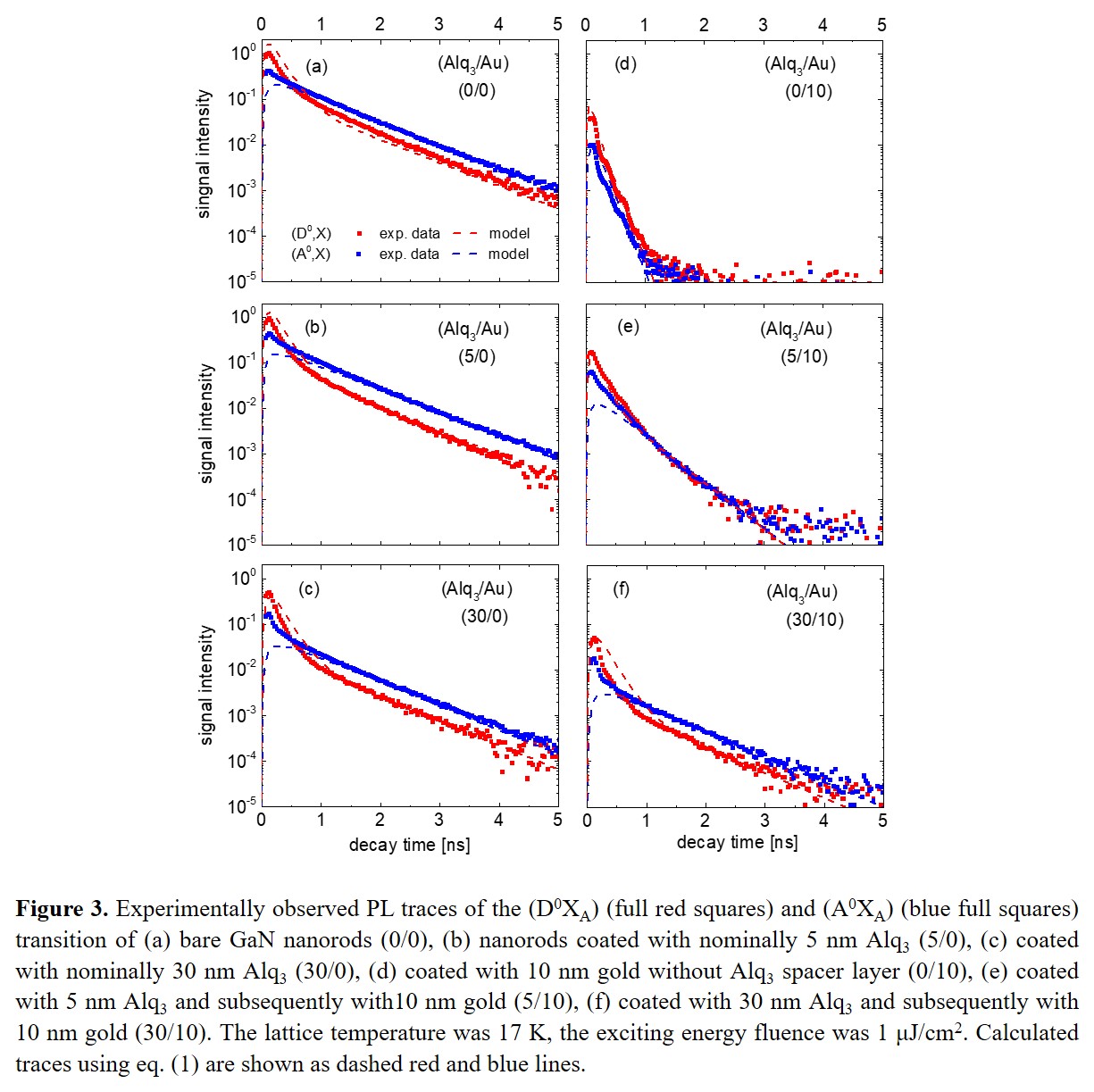
2Reprinted with permission from F. Mohammadi, H. Schmitzer, G. Kunert, D. Hommel, J. Ge, G. Duscher, W. Langbein, and H. P. Wagner, Emission dynamics of hybrid plasmonic gold/organic GaN nanorods, Nanotechnology 28, 505710 (2017), Copyright 2017, IOP.
Effect of Au Substrate and Coating on the Lasing Characteristics of GaAs Nanowires
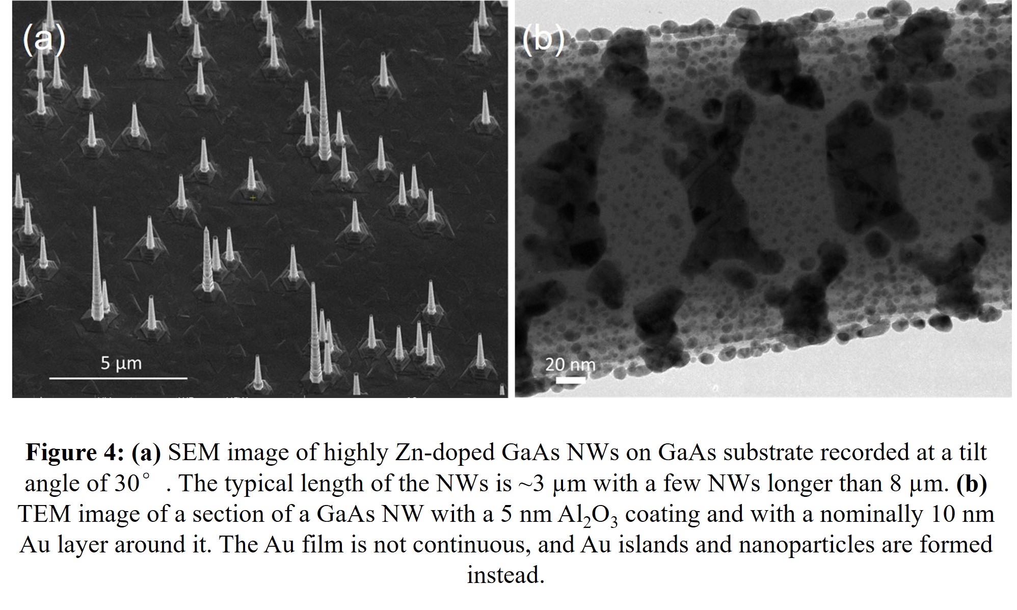
Optically pumped lasing from highly Zn-doped GaAs nanowires lying on an Au film substrate and from Au-coated nanowires has been demonstrated up to room temperature. The conically shaped GaAs nanowires were first coated with a 5 nm thick Al2O3 shell to suppress atmospheric oxidation and band-bending effects. Doping with a high Zn concentration increases both the radiative efficiency and the material gain and leads to lasing up to room temperature. A detailed analysis of the observed lasing behavior, using finite-difference time domain simulations, reveals that the lasing occurs from low loss hybrid modes with predominately photonic character combined with electric field enhancement effects. Achieving low loss lasing from NWs on an Au film and from Au coated nanowires opens new prospects for on-chip integration of nanolasers with new functionalities including electro-optical modulation, conductive shielding, and polarization control.
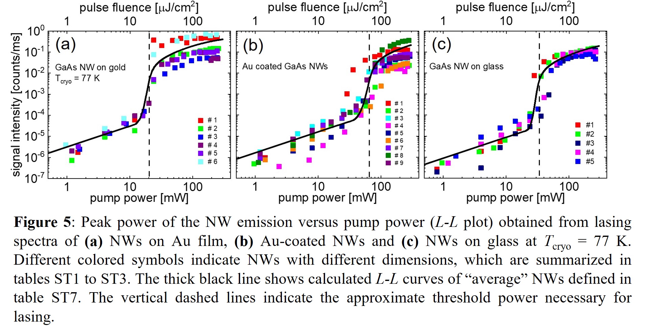
Figs. 4 and 5 reprinted with permission from G. Aman, F. Mohammadi, Martin Fränzl, M. Lysevych, H. Tan, C. Jagadish, H. Schmitzer, M. Cahay, H. P. Wagner, Effect of Au substrate and coating on the lasing characteristics of GaAs nanowires, Scientific Reports 11, 21378 (2021).
Lasing in Zn-doped GaAs nanowires on an iron film
We demonstrated optically pumped lasing in highly Zn-doped GaAs nanowires lying on an iron film. The conically shaped nanowires were first covered with an 8 nm-thick Al2O3 film to prevent atmospheric oxidation and mitigate band-bending effects. Multimode and single-mode lasing have been observed for nanowires with a length greater or smaller than 2 µm, respectively. Finite difference time domain calculations reveal a weak electric field enhancement in the Al2O3 layer at the nanowire/iron film interface for the lasing modes. The high Zn acceptor concentration in the nanowires provides enhanced radiative efficiency and enables lasing on the iron film despite plasmonic losses. Our results open avenues for integrating nanowire lasers on ferromagnetic substrates to achieve new functionalities, such as magnetic field-induced modulation.
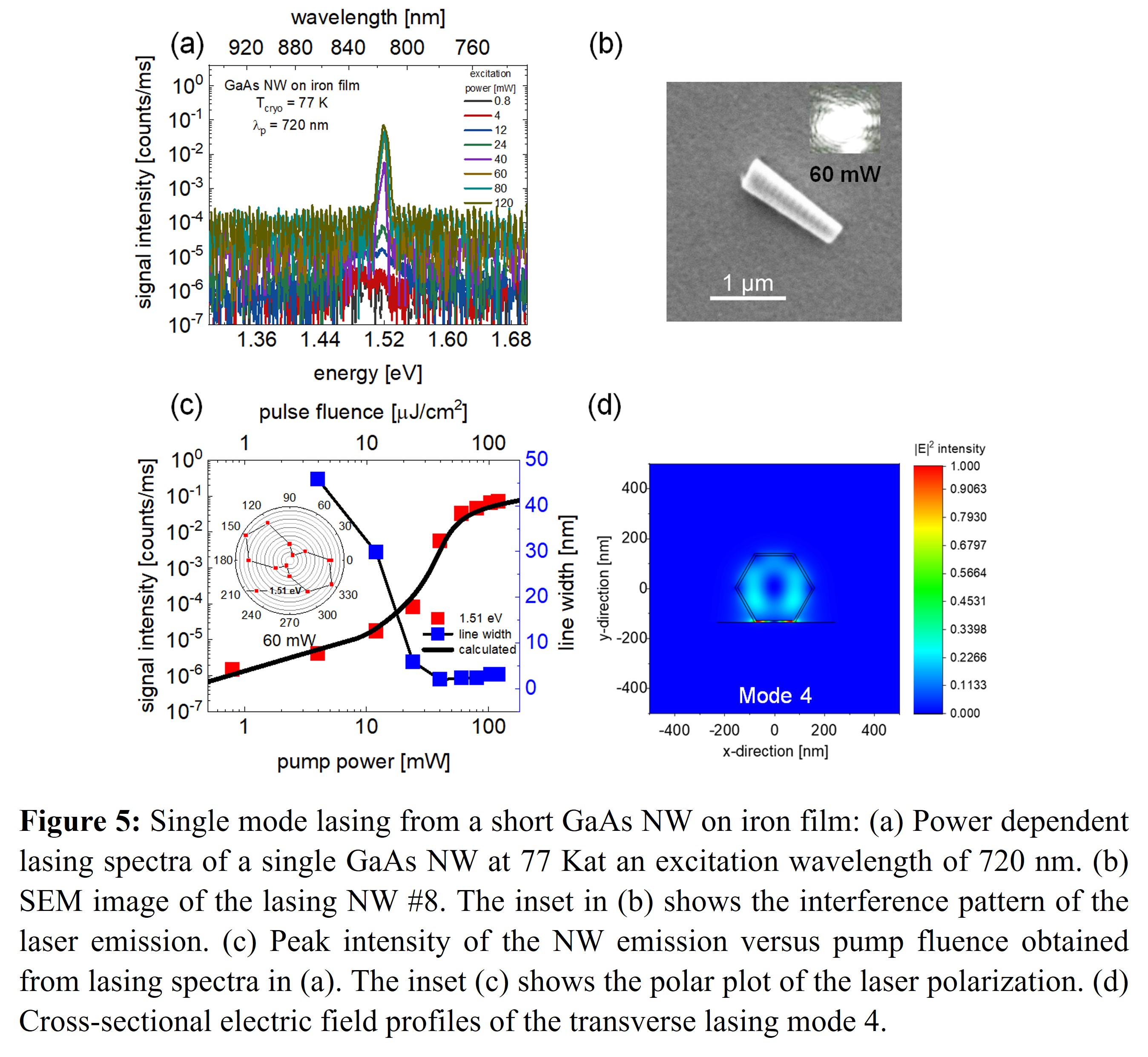
Figure reprinted with permission from G. Aman, Martin Fränzl, M. Lysevych, H. Tan, C. Jagadish, Martin Fränzl, H. Schmitzer, M. Cahay, H. P. Wagner, Lasing in Zn-doped GaAs nanowires on an iron film, Nanotechnology 34, 445201 (2023).