Photonic Nanowire Crystals
Lasing from InP Nanowire Photonic Crystals on InP Substrate
Two-dimensional photonic crystal (PhC) lasing from an InP nanowire array still attached to the InP substrate has been demonstrated for the first time (see Figs. 1 and 2). The undoped wurtzite InP nanowire array was grown by selective area epitaxy and coated with a 10 nm thick Al2O3 film to suppress atmosphere induced oxidation and surface band-bending. The PhC array displays optically pumped lasing at room temperature at a pulsed threshold fluence of 14 μJ/cm2. At liquid nitrogen temperature, the array shows lasing under continuous wave (cw) excitation at a threshold intensity of 500 W/cm2. The output power of the single mode laser line reached values of 470 µW. Rate equation calculations indicate a quality factor of Q ~1000. Investigations near threshold reveal that lasing starts from isolated islands within the pumped region before coherently merging into a single homogenous area with increasing excitation power (see Fig. 3). This field emits a lasing mode with an average off-normal angle of ~6 degrees. Single mode lasing with the nano-array still attached to the InP substrate opens new design opportunities for electrically pumped PhC laser light sources.
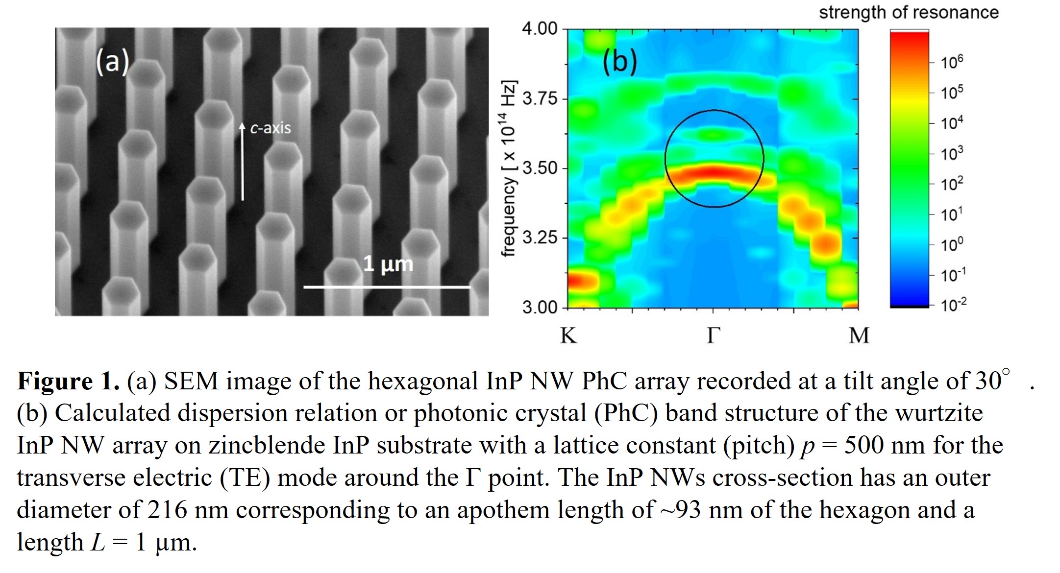
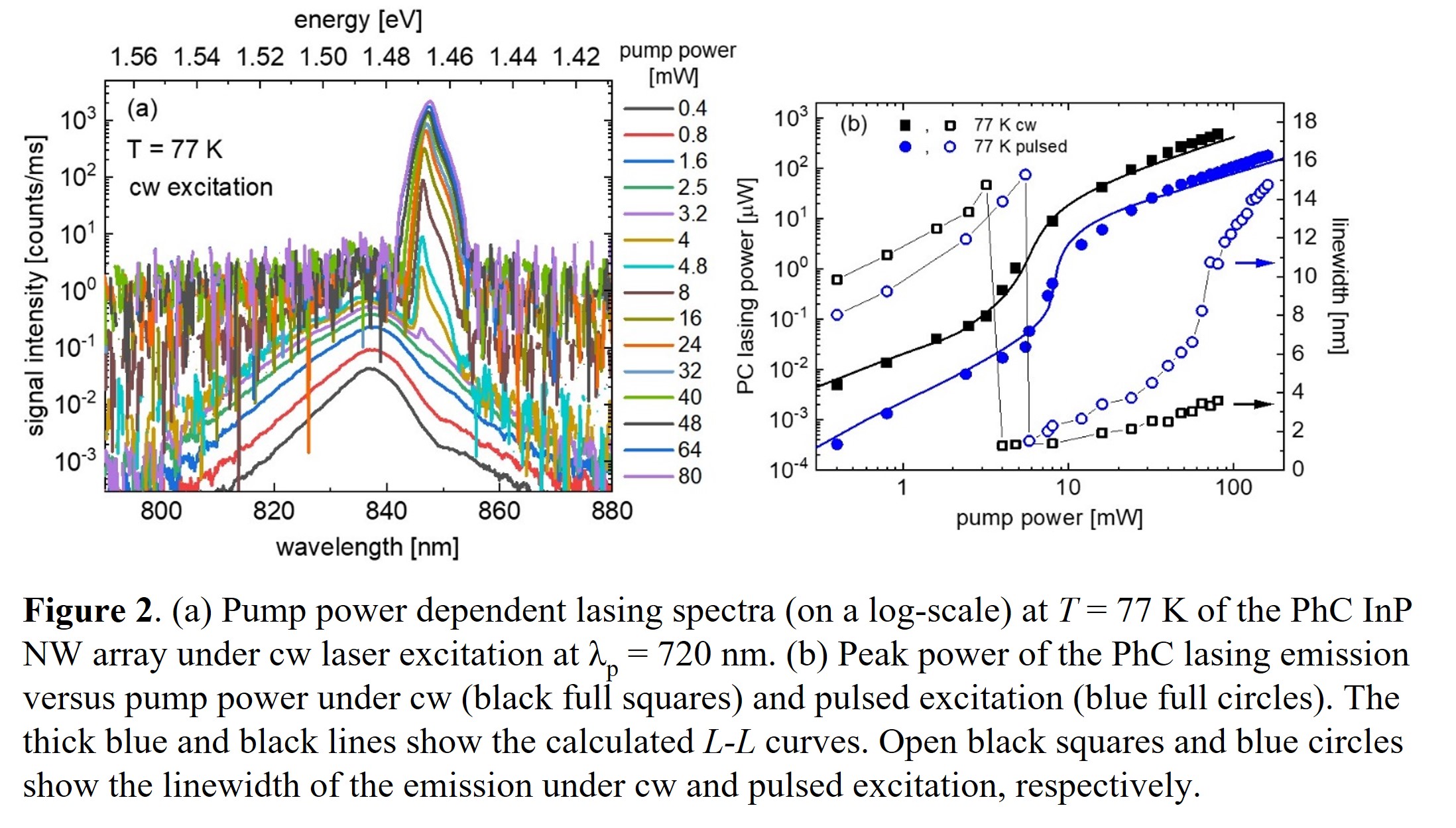
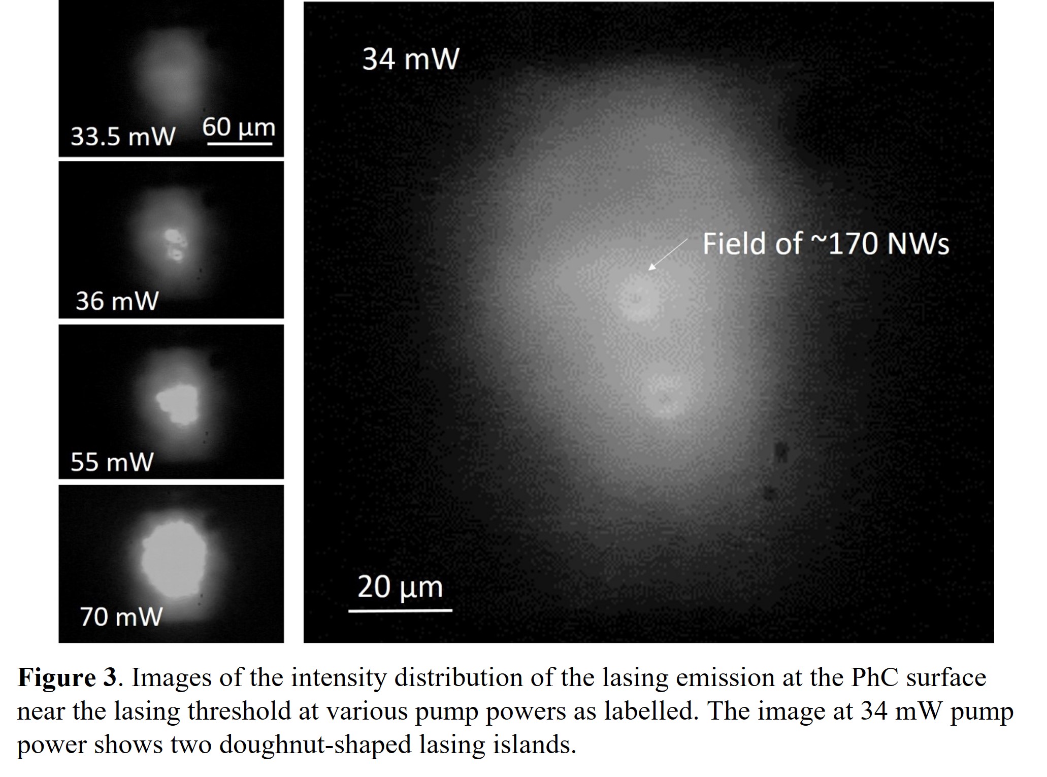
Figures 1-3 reprinted with permission from Chia-Wei Tu, Martin Fränzl, Qian Gao, Hark-Hoe Tan, Chennupati Jagadish, Heidrun Schmitzer, Hans Peter Wagner, Lasing from InP Nanowire Photonic Crystals on InP Substrate, Adv. Optical. Mat. 9, 2001745 (2021), Copyright 2020, Wiley-VCH GmbH.
Reflection from InP Nanowire Photonic Crystals
We demonstrated unique reflective properties of light from bare and gold-coated InP nanowire (NW) photonic crystal arrays. The undoped wurtzite InP nanowire arrays were grown by selective area epitaxy and coated with a 12-nm thick Al2O3 film to suppress atmospheric oxidation. A nominally 10-nm thick gold film was deposited around the NWs to investigate plasmonic effects. The reflectance spectra show pronounced Fabry-Perot oscillations, which are shifted for p- and s-polarized light due to a strong intrinsic birefringence in the NW arrays. Gold-coating of the NW array leads to a significant increase of the reflectance by a factor of two to three compared to the uncoated array, which is partially attributed to a plasmon resonance of the gold caps on top of the NWs and to a plasmonic antenna effect for p-polarized light. These interpretations were supported by finite-difference-time-domain simulations. Our experiments and simulations indicate that NW arrays can be used to design micrometer-sized polarizers, analyzers, and mirrors which are important optical elements in optoelectronic integrated circuits.
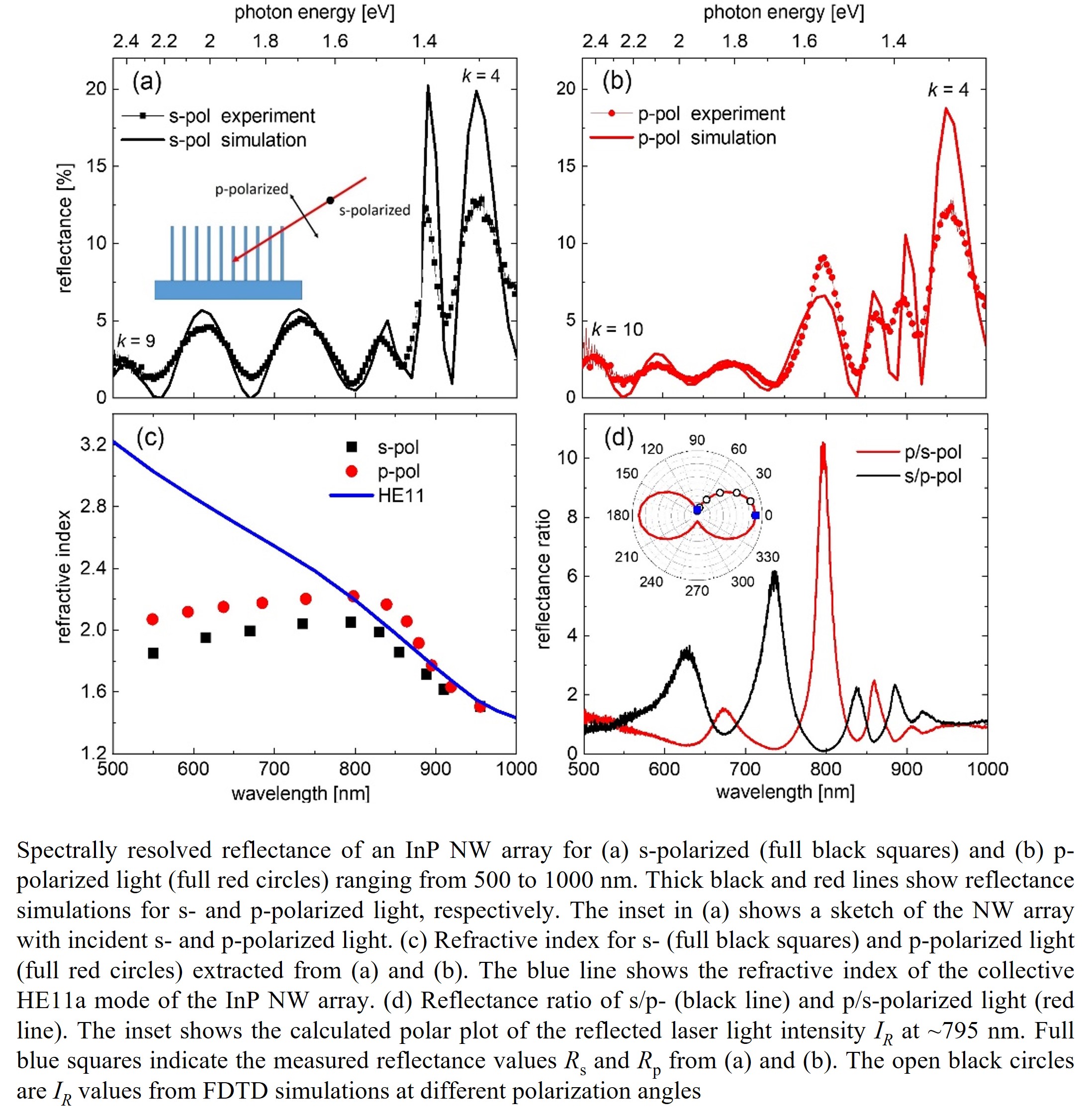
Figure reprinted with permission from Chia-Wei Tu, Masoud Kaveh, Martin Fränzl, Qian Gao, Hark-Hoe Tan, Chennupati Jagadish, Heidrun Schmitzer, Hans Peter Wagner, Unique reflection from birefringent uncoated and gold-coated InP nanowire crystal arrays, Opt. Express 30, 3172-3182 (2022), Copyright 2022, OSA.
Polarization Conversion of Light Diffracted from InP Nanowire Photonic Crystal Arrays
We investigated the polarization state of light diffracted from uncoated and gold-coated InP nanowire photonic crystal arrays grown by selective area epitaxy. Experimental data and finite-difference time-domain simulations show that both the intensity and the ellipticity of the polarization state of the diffracted light beam can be controlled by the nanowire dimensions and gold coating, while the diffracted angle remains unchanged with respect to variations of these parameters. A nominally 10 nm-thick gold film deposited around the nanowires enhances the diffraction intensity by plasmonic effects. Our results demonstrate that the controlled conversion of incident linearly polarized light to circularly polarized or rotated linearly polarized diffracted light can find applications in photonic integrated circuits. The high sensitivity of the polarization state with respect to alterations of the nanowire dimension opens new prospects in the areas of semiconductor metrology and microchip inspection as well as for submicron particle detection.
Figure reprinted with permission from Chia-Wei Tu, Masoud Kaveh, Martin Fränzl, Qian Gao, Hark-Hoe Tan, Chennupati Jagadish, Heidrun Schmitzer, Hans Peter Wagner, Lasing from InP Nanowire Photonic Crystals on InP Substrate, Adv. Optical. Mat. 11, 2202342 (2023), Copyright 2023, Wiley-VCH GmbH.