University of Cincinnati
ECE&CS Department
EE-612
Microwave Communication Lab.
Prepared by: Prof.Altan M. Ferendeci
Experiment #5
Measurement of the Noise Figure of a Transistor
Purpose:To measure the noise figure of a transistor at microwave frequencies and find the appropriate noise figure parameters of a transistor. To find the variation of minimum noise figure as a function of frequency and bias points.
Instrument Noise Figure Meter, Noise Source.
Theory
Noise figure is an important parameter in designing initial stages of communication circuits. The smaller the noise figure of a transistor, the better will be sensitivity of the receiver and the lower will be the minimum detectable signal level.
At a given frequency, the three noise figure parameters that are needed for transistor amplifier design are
- minimum noise figure Fmin,
- corresponding source admittance Yo=Go+jBo and
- equivalent normalized noise resistance rn = Rn/Zo.
Once these are known, the noise figure corresponding to any other source admittance can be calculated from
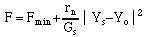
Here Gs is the conductance term of the source admittance Ys.
Experiments
Set the experiment as shown in the figure. Bias to the transistor is applied through the bias tees. Be sure that you do not break the dc path while adjusting the line stretcher.
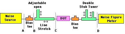
- With a matched load connected to the bias network, measure the impedance of the bias network at various frequencies using the slotted line.
- Remove the system from A and D. Connect the noise source and the noise figure meters together and calibrate the noise figure meter.
- With proper bias applied to the transistor, adjust the double stub tuner for maximum output power reading.
- Adjust the line stretcher and the adjustable open for minimum noise figure reading. Once this is achieved, turn the transistor power off, disconnect at C and measure the source impedance with the slotted line. For this measurement you can replace the noise source with a matched load.
- Remove the input tuning circuit and measure the noise figure with bias network connected directly to the DUT (B and C connected together).
- Repeat these measurements for various collector currents at a given frequency and at a constant VCE voltage.
Bias Conditions:
- 3 V, 20.0 mA
- 3 V, 40.0 mA
- Repeat these measurements for different frequencies (2, 5 and 10 GHz) at the given bias points.
- Plot the following curves:
- Fmin vs Id(mA) at a given frequency and VDS, and
- Fmin vs freq at a given bias point
- Discuss the possible errors in the measurements.
Reference: Microwave Transistor Amplifiers, G. Gonzalez, Prentice Hall, 2nd Edition (1997).
Goto Homepage