Goal:
To Design a Microwave Amplifier
Using S-parameters of a Transistor
The final amplifer block diagram is shown in the figure below.
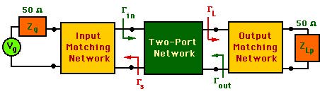
Various blocks represent
- Vg = Signal generator voltage
- Zg = Signal generator internal impedance (usually 50 W but can be a complex impedance from another sourse)
- Input Matching Network
- Two port network representing the transistor
- Output Matching Network
- Zlp=Output (Load) Impedance (usually 50 W but can be a complex load impedance)
The block diagram above can be simplified into the following form:
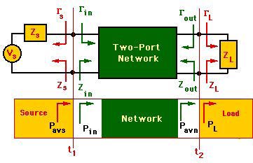
- The Generator Voltage Vg is replaced by a Thevenin equivalent source voltage Vs.
- The Generator Impedance Zg is transformed into a complex source impedance Zs with an equivalent reflection coefficient Gs transformed by the Input Matching Network.
- The Load ZLpis transformed into a single complex load impedance ZL with an equivalent reflection coefficent GL transformed by the Output Matching Network.
These two parameters play a very important role in determining the overall gain of the amplifier. Also the source impedance determines the noise figure of the amplifier.
The lower block diagram is used in definitions associated with various gains of the amplifier.