ECECS 349
Measurements Laboratory
Experiment #1
Part B
PSPICE Circuit Simulations
OBJECTIVE
The objective of this lab is
to become familiar with the PSPICE circuit simulation program. The program is installed
on all PCs in the lab. Attention should be focused toward using the schematics
software. The software allows you to design and analyze complicated analog
circuits containing components such as resistors, capacitors, inductors,
diodes, transistors, and many others.
The PSPICE software will be used in future labs and it is therefore
important for you to become familiar with all its capabilities.
Here is a listing of
tutorials URL for the PSPICE:
http://search.yahoo.com/search?p=%22pspice%2Btutorial%22&fr=FP-tab-web-t&toggle=1&cop=&ei=UTF-8
(or you can search for
“Pspice+tutorial”)
In this lab, PSPICE will be
used to perform DC Analysis, Transient Analysis, and AC Analysis of simple
networks which have been studied theoretically in other classes (Network
Analysis). Whenever possible, you should
compare the results obtained from your PSPICE simulations with the theoretical
results which were discussed in class or in previous courses. During this lab, you will simulate a DC
resistance network via DC analysis and simulate the charging of a capacitor in
the time domain. Further, you will analyze a low pass filter in the frequency
domain producing its Bode plot.
Note :
(1) Make sure to save or print all the plots you
obtained while completing this assignment.
(2) Whenever possible you must include the
theoretical calculations in the analysis of the different circuits and compare
them to your PSPICE results.
Problem #1: DC
Analysis
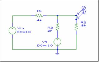
(a) Calculate
(by hand) the current through R2 using Kirchoff’s law.
(b) Verify your prediction using a computer
simulation. (show a plot with I and V markers)
(c) Plot the voltage drop across R2 with DC
analysis (DC Sweep) while Vin is varied from 1V to 10V
Problem #2:
Transient Analysis
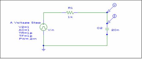
This PSPICE circuit will simulate the transient
response of a series RC network. The input pulse (transient) will be generated
from a simulated step voltage source called VPULSE. You will observe the
capacitor charging after the positive step of the pulse and the capacitor
discharging after the negative step.
The circuit to b
analyzed is shown on the diagram above.
Use R1 = 1 KW and C2 =20 nF (0-1V step)
(a) Calculate an appropriate
time scale to show the complete charging or discharging of the capacitor (5-10
time constants , t=RC)
(b) Choose an appropriate shape
(rise time, fall time and pulse width) of the VPULSE source to show the full transient charging
and discharging of the capacitor. An appropriate time scale is shown below.
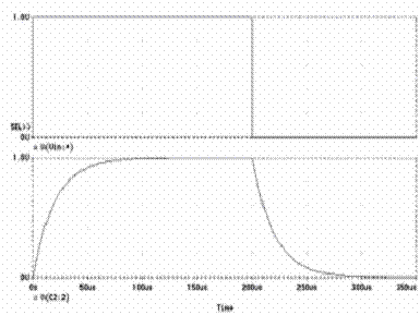
(c) When the
parameters have been calculated, plot the graph of the voltage as a
function of time across the capacitor.
(d) In your
lab report describe the steps taken to obtain the display.
Problem #3:
Frequency Response and Bode Plot
For the
circuit shown above (Problem 2)
(a) Plot Vout (the voltage
across the capacitor) versus frequency over a frequency range which shows the
roll off above the break frequency of the filter. As shown below:
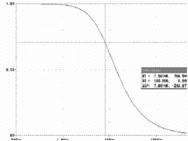
(b) From the data file (or from
the plot) of Vout as a function of frequency, determine the -3dB point, i.e.,
the break frequency. How does your value
compare with the theoretical value given in class (calculate the % error). The
-3dB should occur at f=1/2pRC
(c) What type of filter is this
simple RC network? Explain.
(d) How would you build a high-pass filter using
a resistor and an inductor? Explain.